Methods Used in Prototype Circuit Board Assembly
Printed circuit boards (PCBs) provide the mechanical structure and electrical connections for devices ranging from consumer electronics to industrial equipment. As electronic devices become increasingly complex, effective PCB inspection is vital to ensuring high quality and reliability. This article examines the main inspection methods used in prototype circuit board assembly to identify defects before they go into production.
Manual visual inspection is a traditional method that involves skilled operators manually inspecting PCBs for physical defects. While this can be useful for detecting obvious problems, such as solder bridges and missing components, it can miss issues that are harder to detect with automated inspection techniques, such as AOI and X-ray. As such, a combination of visual inspection and automated inspection is often used to ensure a thorough PCB inspection process.
Automated optical inspection (AOI) uses cameras to automatically check PCBs for defects, ensuring that the finished product is free from errors that could lead to poor performance or failure. AOI systems can inspect for things like component placement, solder joint quality, and labeling. They can also inspect for misalignments, solder voids, and other defects. Some AOI systems use two-dimensional imaging to scan a PCB from different angles, while others use three-dimensional imaging for more detailed inspection.
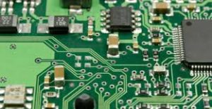
Inspection Methods Used in Prototype Circuit Board Assembly
Functional testing is a crucial step in prototype PCB assembly, applying power and signals to the circuit to simulate its operation. This allows engineers to see how the prototype behaves under real-world conditions and can help them spot any areas that may require improvement or repair. Functional tests can include everything from simple on/off power test to in-depth testing using specialized software.
Other types of PCB testing and inspection include bare PCB electrical testing, which checks the circuit board for defects before it is assembled. This can detect things such as open circuits and short circuits, which are usually caused by mistakes in the PCB etching or soldering processes. It can also evaluate the conductivity of individual traces, pads, and vias to make sure they are functioning properly.
PCBs can also undergo environmental testing to evaluate their ability to withstand varying temperatures, humidity levels, and vibration. This can help identify any potential reliability issues and prevent them from being discovered during the manufacturing and assembly process.
Finally, X-ray inspection is a non-contact, nondestructive technique that can check the inner layers of a PCB for hidden defects. This can reveal issues that other inspection methods might miss, such as voids in solder joints or problems with internal traces. X-rays work by assessing the atomic weight of materials, with heavier elements such as solder absorbing more X-rays than lighter ones. This allows engineers to quickly and accurately pinpoint defects without removing the prototype from the production line. X-ray inspection is a more expensive alternative to other inspection methods, but it can be worth the investment for high-volume production.