Hdi printed circuit board Materials
The evolution of High-Density Interconnect (HDI) printed circuit boards (PCBs) has been marked by continuous advancements in materials technology. HDI boards, known for their compact size, high interconnect density, and enhanced performance, have become indispensable components in a wide range of electronic devices. This article explores the latest innovations in HDI PCB materials and their implications for the electronics industry.
One of the key areas of innovation in HDI PCB materials is the development of advanced substrates with superior electrical, thermal, and mechanical properties. Traditionally, PCBs have been manufactured using materials such as FR-4 (Flame Retardant 4) and polyimide, which offer good overall performance but may not meet the stringent requirements of high-speed and high-frequency applications. Newer substrates, such as liquid crystal polymer (LCP), PTFE (Polytetrafluoroethylene), and high-speed laminates, address these challenges by providing lower dielectric loss, higher thermal conductivity, and improved signal integrity, essential for emerging technologies like 5G, IoT (Internet of Things), and autonomous vehicles.
Moreover, advancements in substrate manufacturing techniques, such as laser-drilling and sequential build-up (SBU), enable the fabrication of ultra-thin dielectric layers and finer feature sizes, pushing the limits of miniaturization and high-density interconnectivity in hdi printed circuit board. These innovations facilitate the integration of complex circuitry into smaller form factors, allowing for more compact and lightweight electronic devices with improved performance and functionality.
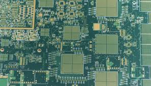
Innovations in Hdi printed circuit board Materials
In addition to substrates, the choice of conductive materials used in HDI PCBs has also undergone significant innovation. Traditional PCBs rely on copper for conductive traces and vias, but the demand for higher data rates and increased reliability has led to the development of alternative materials with superior electrical conductivity and reliability. Silver, for example, offers lower resistance and better solderability compared to copper, making it an attractive choice for high-frequency applications where signal integrity is critical.
Furthermore, the introduction of advanced plating techniques, such as electroless nickel immersion gold (ENIG) and electroplated palladium nickel (ENEPIG), enhances the performance and reliability of HDI PCBs by providing superior corrosion resistance, solderability, and wire bonding capabilities. These plated finishes not only improve the longevity of electronic components but also ensure robust interconnectivity and compatibility with lead-free soldering processes, aligning with environmental regulations and industry standards.
Another area of innovation in HDI PCB materials is the development of environmentally friendly alternatives to traditional solder masks and surface finishes. With growing concerns about the environmental impact of electronic waste, there is increasing demand for eco-friendly solutions that minimize the use of hazardous substances and promote recyclability. Bio-based solder masks, made from renewable sources such as plant-derived resins, offer a sustainable alternative to conventional materials without compromising performance or reliability.
Moreover, the adoption of lead-free surface finishes, such as organic solderability preservatives (OSP) and immersion silver (ImAg), reduces the environmental footprint of HDI PCB manufacturing while ensuring compliance with regulatory requirements, such as the Restriction of Hazardous Substances (RoHS) directive. These innovations reflect a broader shift towards sustainable practices in the electronics industry, where environmental considerations are becoming increasingly important.
In conclusion, innovations in HDI printed circuit board materials are driving progress and pushing the boundaries of what is possible in electronic design and manufacturing. From advanced substrates and conductive materials to eco-friendly surface finishes, these advancements enable the development of smaller, faster, and more reliable electronic devices with reduced environmental impact. As technology continues to evolve, the pursuit of novel materials and manufacturing techniques will remain central to the ongoing success and sustainability of the electronics industry.